You have 0 items in your cart.
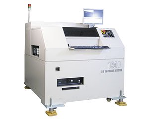
Detection of IC lead pseudo-contact (poor contact) states
• High-speed testing at up to 0.025 sec./step (1240-01, 1240-03)
• Detection of IC lead float and pseudo-contact states
• Support for active testing (optional feature)
• High-precision probing
• Large testing area of 510 × 460 mm (1240-01, 1240-02)
• Standard transport capability
• Automatic alignment function and simple visual test function
■ Specifications overview
| 1240-01, 1240-02 | 1240-03 | |
| Number of arms | 4 (L, R, ML, MR) | |
| Number of test steps | 40,000 (max.) 300,000 (optional feature) |
|
| Measurement ranges | Resistance: 400 μΩ to 40 MΩ Capacitance: 1 pF to 400 mF Inductance: 1 μH to 100 H Diode VZ measurement: 0 to 25 V Zener diode VZ measurement: 0 to 25 V, 25 to 80 V (optional feature) Digital transistors: 0 to 25 V Photo couplers: 0 to 25 V Short: 0.4 Ω to 400 kΩ Open: 4 Ω to 40 MΩ DC voltage measurement: 0 to 25 V |
|
| Measurement time | Max. 0.025 sec./step (X-Y 2.5 mm movements, Z height of 5 mm, simultaneous probing of 3 steps, S/O measurement) |
|
| Probing precision | Within ±100 μm for each arm (X and Y directions) | |
| Positioning repeatability | Within ±50 μm (probing positions) | |
| Inter-probe pitch | Min. 0.2 mm (when using needle probes) Min. 0.5 mm (when using 4-terminal probes) |
|
| Probe working area | 510 mm (20.08 in) W × 460 mm (18.11 in) D | |
| Testable board dimensions | Thickness: 0.6 mm (0.02 in) to 3.2 mm (0.13 in) Outer dimensions: Min. 50 mm (1.97 in) × 50 mm (1.97 in), max. 510 mm (20.08 in) × 460 mm (18.11 in) |
|
| Power supply | 200 V AC ±10% (single-phase), 50/60 Hz, 3 kVA | |
| Dimensions and mass | 1410 mm (55.51 in) H × 1340 mm (52.76 in) H × 1270 mm (50.00 in) D, 1300 kg (45,855.4 oz) | 1260 mm (49.61 in) H × 1300 mm (51.18 in) H × 1200 mm (47.24 in) D, 1050 kg (37,037.0 oz) |


